Semiconductor manufacturing is arguably the most demanding environment in which any mechanical component can be asked to operate. The positioning tolerances required are measured in nanometres. The cleanliness standards — typically ISO Class 1 to ISO Class 4 cleanrooms — permit only a handful of particles per cubic metre of air. The chemical environment includes corrosive process gases, ultra-pure water, and aggressive solvents. And the consequence of contamination or positioning error is not a cosmetic defect but the destruction of a silicon wafer worth thousands of dollars, or the compromise of an entire fabrication lot.
In this environment, every mechanical component in a motion system is scrutinised for particle generation, outgassing, chemical compatibility, and positional accuracy. The Oldham-Kupplung survives this scrutiny because its unique combination of zero backlash, zero bearing load, electrical isolation, and availability in ultra-low-outgassing materials satisfies requirements that no other common coupling type can meet simultaneously. This article examines the specific applications, material requirements, and performance standards that govern Oldham coupling specification in semiconductor equipment.
The Cleanroom Contamination Challenge
A single particle larger than 0.1 microns landing on a wafer surface during photolithography can cause a critical defect in the integrated circuit being fabricated. A molecule of outgassed organic compound from a polymer component can deposit on the wafer surface and alter the surface energy in ways that affect photoresist adhesion, etch uniformity, or thin-film deposition. These are not theoretical concerns — they are the day-to-day contamination management challenges of semiconductor process engineers.
Every mechanical component in the wafer handling path — robots, linear stages, rotary stages, and the couplings connecting their drives — must be evaluated for:
- Particle generation rate: How many particles of defined size does the component shed per unit time during normal operation? This is measured in a controlled chamber and expressed as particles per minute per unit area or volume.
- Outgassing rate: What is the rate of volatile organic compound (VOC) emission from the component at operating temperature in vacuum or near-vacuum conditions? Measured in Pa·m³/s per unit area, this parameter governs the suitability of materials for use in vacuum process chambers.
- Chemical compatibility: Does the material resist the process chemicals present in its operating zone — hydrogen fluoride vapour, ozone, isopropyl alcohol, ammonium hydroxide, hydrogen peroxide, and others depending on the process step?
- Ionic contamination: Does the material release metallic ions or other ionic species that could deposit on wafer surfaces and alter device electrical characteristics?
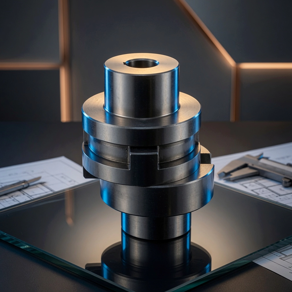
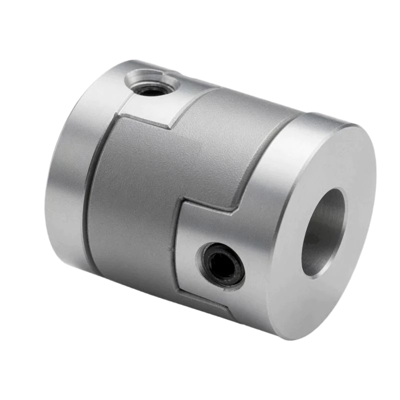
Why the Oldham Coupling’s Sliding Disc Is Both the Challenge and the Solution
The centre disc’s sliding motion is the source of the Oldham coupling’s misalignment accommodation capability — but it is also a potential source of particle generation. Every sliding contact produces wear debris, and in a cleanroom environment those debris particles must be managed.
The key is material selection. Standard acetal generates measurable particles during operation that are acceptable in industrial environments but too high in particle count and size distribution for ISO Class 3 or better cleanroom use. PEEK, and in particular PEEK filled with PTFE or carbon fibre, generates substantially fewer and smaller particles under the same sliding conditions, with a particle size distribution that falls more favourably against cleanroom classification standards.
For the most demanding semiconductor applications — inside process chambers or in ISO Class 1 to 2 environments — ultra-clean PEEK grades with controlled purity (low metallic ion content, no plasticisers or fillers that could outgas) are specified. These materials are manufactured under controlled conditions with documented lot-to-lot consistency in outgassing rates and particle generation profiles. The cost is significantly higher than standard PEEK, but the qualification data package they come with is essential for equipment manufacturers seeking process tool approval from chipmakers.
Wafer Handling Robot Joints
Atmospheric wafer handling robots — the SCARA and Cartesian robots that transfer wafers between cassettes, load locks, and process chambers — have multiple rotary joints, each driven by a servo motor through a harmonic drive or gear reducer. The coupling between the motor output shaft and the harmonic drive input is an Oldham coupling in most modern designs.
The requirements here are exacting. The robot must position a 300 mm wafer to within ±0.1 mm at the process chamber entrance slot, repeated millions of times over the tool’s service life. Any coupling backlash at the joint produces an end-effector positioning error amplified by the robot’s kinematic chain. Zero backlash at every joint is a non-negotiable requirement.
The lateral offset tolerance of the Oldham coupling absorbs the small but unavoidable shaft misalignments between the motor and harmonic drive in the compact, stacked joint assembly — misalignments that cannot be corrected by shimming in the confined space of a robot joint housing. The alternative — a bellows coupling — would impose radial loads on the harmonic drive’s input bearing, reducing its service life in a component that is expensive and time-consuming to replace in a robot that may be installed in a process tool under a multi-year service contract.
Linear Precision Stages
Photolithography steppers and scanners, wafer inspection systems, and metrology tools use ultra-precision linear stages with positioning resolution in the nanometre range. The stage is driven by a linear motor or a ballscrew, with a servo control loop closing on a laser interferometer or optical encoder reading. Any mechanical compliance or backlash in the drive chain directly appears as positional error in the feedback loop.
In ballscrew-driven precision stages, the Oldham coupling between the servo motor and the ballscrew serves the same function as in any CNC machine — zero-backlash torque transmission with lateral offset accommodation — but to higher performance standards. The coupling must maintain zero backlash for the full qualified service life of the stage, typically 5 to 10 years of daily use, with disc replacement performed as part of the stage’s planned maintenance schedule. Precision-grade Oldham couplings for these applications are manufactured to tighter tenon width tolerances than standard industrial couplings, minimising the initial backlash from assembly tolerance stack-up.
Vacuum Compatibility: A Critical Additional Requirement
Many semiconductor process steps occur in vacuum — physical vapour deposition, chemical vapour deposition, ion implantation, and etch processes all operate at pressures ranging from atmospheric down to 10⁻⁹ Torr. Mechanical components in or near vacuum chambers must not outgas at rates that compromise the process vacuum.
Standard polymer materials — including standard-grade acetal, nylon, and even standard PEEK — contain residual monomers, plasticisers, and processing aids that outgas in vacuum at rates unacceptable for high-vacuum semiconductor processes. Vacuum-compatible PEEK grades are manufactured with controlled outgassing rates, typically meeting NASA outgassing standards (ASTM E595): total mass loss below 1.0 percent and collected volatile condensable material below 0.1 percent after 24 hours at 125°C in vacuum.
For Oldham couplings used in vacuum environments, specify disc materials with documented outgassing data from the manufacturer. Standard catalogue couplings are not vacuum-rated; vacuum-compatible versions require specific material certification and often bakeout procedures before installation in the process chamber environment. Hub materials for vacuum applications are typically 304 or 316L stainless steel with electropolished surfaces — the low surface area-to-volume ratio of the polished surface minimises the adsorbed gas layer that desorbs in vacuum.
Electrical Considerations in Semiconductor Equipment
Semiconductor wafers are electrostatically sensitive — charge accumulation on the wafer surface during handling can damage gate oxide layers with electrostatic discharge (ESD) events that leave no visible mark but destroy device functionality. Equipment grounding and electrostatic management are engineering disciplines in their own right in semiconductor tool design.
The Oldham coupling’s electrical isolation property — provided by the non-conducting polymer disc — prevents shaft currents generated by servo drive switching from propagating through the drive chain into the robot structure and potentially to the wafer. In some tool designs, this isolation is deliberately engineered into the drive train using an Oldham coupling specifically to break the electrical continuity between the servo amplifier and the robot’s conductive end-effector and wafer handling surfaces.
Conversely, in tools where the robot structure must be grounded throughout for ESD management, a metallic coupling is specified to maintain electrical continuity. The coupling specification must match the equipment’s grounding architecture, which requires understanding the tool’s ESD management strategy before selecting between polymer-disc and metal-disc Oldham couplings.
Specification Checklist for Semiconductor Oldham Couplings
| Requirement | Spezifikation | Rationale |
|---|---|---|
| Disc material | Ultra-clean PEEK or PTFE composite | Low particle generation, low outgassing, chemical resistance |
| Hub material | 316L stainless steel, electropolished | Corrosion resistance, low adsorbed gas layer, cleanroom-compatible surface |
| Outgassing certification | ASTM E595 (TML <1.0%, CVCM <0.1%) | Required for vacuum process environments |
| Hub style | Clamp (split bore) | No shaft surface damage, repeatable concentricity, no set screw particle risk |
| Lubrication | None (dry running) | Lubricant vapour is a contamination source in cleanroom and vacuum environments |
| Backlash | Zero (0 arc-minutes nominal) | Wafer positioning accuracy requirements |
| Cleaning compatibility | IPA, DI water wipe-down | Standard cleanroom component cleaning procedure |
Abschluss
Semiconductor equipment represents the most technically demanding operating environment that an Oldham coupling encounters anywhere in its application range. The combination of nanometre-level positioning requirements, sub-micron particle generation limits, vacuum outgassing standards, ESD management requirements, and aggressive chemical compatibility demands would eliminate most coupling types from consideration entirely. The Oldham coupling survives this qualification process — when specified with the correct ultra-clean PEEK disc, electropolished stainless hubs, and documented outgassing certification — because its operating principle produces zero bearing load, zero backlash, and dry running, all of which align precisely with what semiconductor process environments require. The engineering investment in correct specification at the design stage is repaid many times over in reduced wafer loss, extended tool uptime, and simplified cleanroom maintenance procedures.
Contact our engineering team for semiconductor-grade Oldham coupling specifications including outgassing documentation, or browse our precision coupling range for cleanroom applications.


